Part 2 – MRAM in 22FFL
The second 22FFL paper at IEDM18 [1] describes the integration of Magnetic Tunnel Junction (MTJ)-based MRAM (magnetic random-access memory) into the back-end of the process. MTJ technology is attractive for embedded non-volatile memory because of relatively low cost compared with e-flash, with comparable endurance and data retention properties.
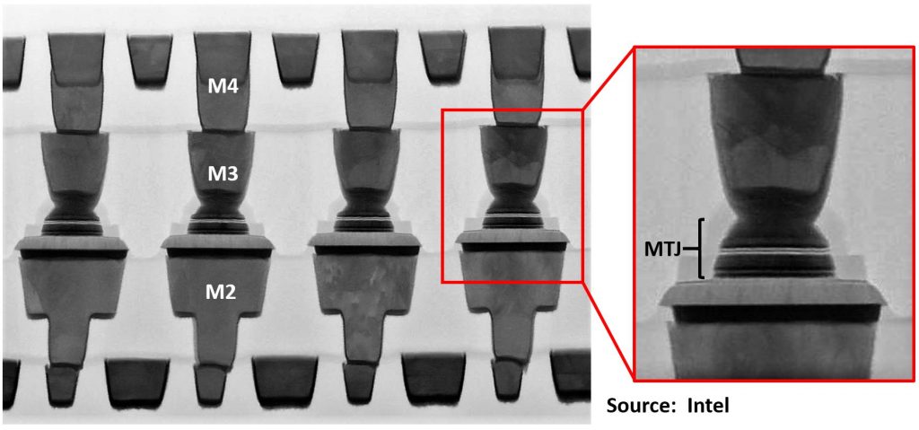
Intel’s MRAM memory cells are built from dual-MgO MTJs, separated by a CoFeB-based free layer in a 1 transistor-1 resistor (1T-1R) configuration between metal 2 and metal 4, shown in this TEM image:
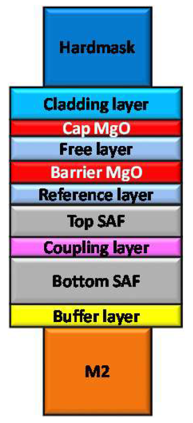
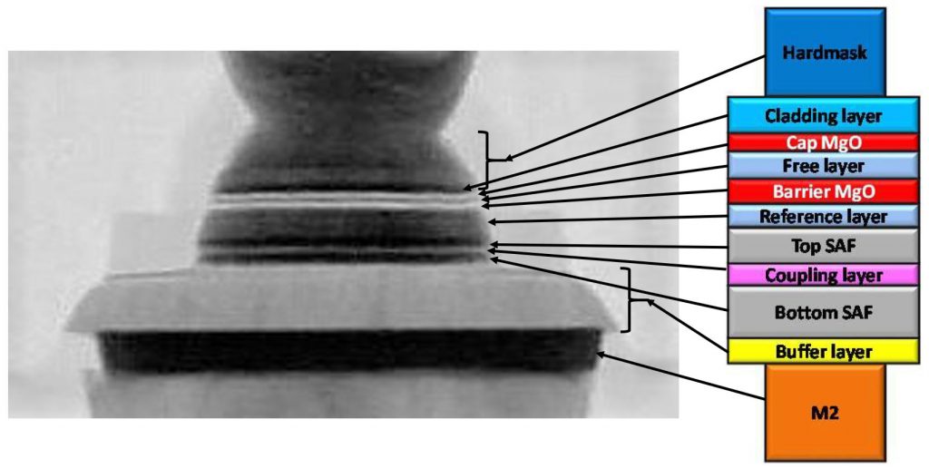
A schematic cross-section of the MTJ stack was also shown:
Data storage in an MTJ relies on the Perpendicular Magnetic Anisotropy (PMA) created by interfacial anisotropy between the MgO and CoFeB layers; placing the free layer between two MgO interfaces enhances the anisotropy and hence data retention. The magnetic state of the free layer can be switched to be parallel (P) or anti-parallel (AP) to the reference layer; if it is parallel, we have low resistance (RP), if anti-parallel, higher resistance (RAP). Switching is done by forcing a current in one direction to go from P to AP, and in the reverse direction to go from AP to P.
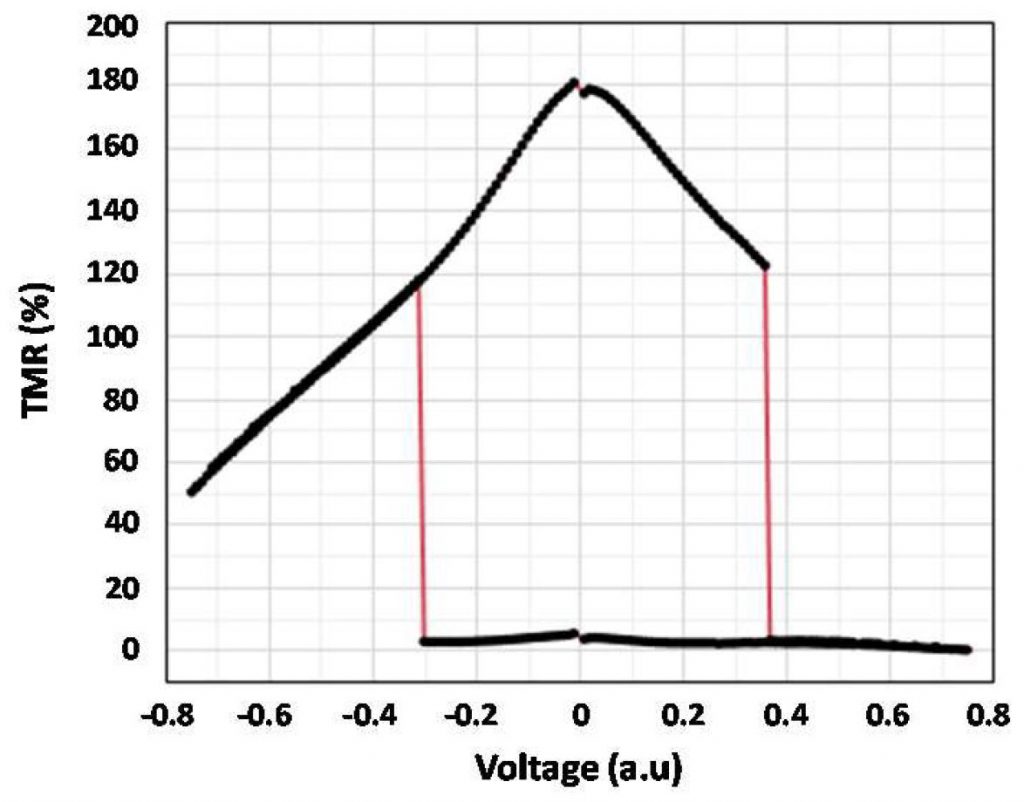
Two parameters used to characterize MTJs are the Tunneling Magneto-resistance Ratio (TMR) and Resistance-Area Product (RA). The latter is what it says, the multiple of the MTJ area and its resistance; TMR is given by (RAP – RP)/ RP, usually as a percentage, and the higher the TMR, the better the read margin for the memory cell. In this paper the RA is 9 ?µm2, and the TMR over 180%. A typical TMR-vs-Voltage curve, showing the hysteresis given by the magnetic switching of the free layer, looks like:
The layout and equivalent circuit of the 1T-1R cell used by Intel is shown below:
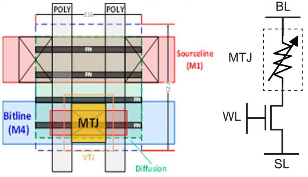
The MTJ is on a Metal 2 pad, on a 216 nm x 225 nm grid (2 x gate pitch, 5 x fin pitch), giving a cell area of 0.0486 um2 (for comparison, the 22FFL SRAM cell is 0.088 um2). Since we have scale bars, we can see that drawn gate length is ~40 nm, and confirm that poly pitch in the cell is the stated ~108 nm, and fin pitch is the design ~45 nm. There appear to be four fins in the cell, so gate width is ~330 nm. And of course, even though the gates are labeled POLY, the final product gate will be HKMG.
The cell layout has an unusual feature in that the M1 sourceline and M4 bitline are parallel; normally in logic areas they would be perpendicular to each other. Another oddity is in the TEM image above – even though the layout seems to show the MTJ being in a vertical stack above the fin, there is no contact or via below M1 to connect to the source/drain of the wordline. The paper describes the TEM image in its “Test Vehicle” section, so it may be of a test die for evaluating the MTJ stack rather than cell function.
If we zoom in on the stack itself, it is tempting to try and correlate the image layers with the schematic, though not being an MRAM expert this is pure speculation;
Of course, an image like this tempts me to hypothesize about a fabrication sequence, and this is what I have come up with:
- Dual-damascene M2
- W cap, mask & etch
- Dielectric deposition & CMP to expose W
- Buffer layers, MTJ stack & hard-mask (TiN (?), also top electrode?) deposition
- Anneal
- Mask & etch MTJ stack down to buffer layers (ion beam etch?)
- Dielectric cap deposition (SiON?)
- Mask & etch buffer layers, overetch into dielectric on ILD2
- ILD3 deposition
- Via 3 pattern & etch through dielectric cap on MTJ to top electrode
- Form M3 barrier layers
- Mask to expose MTJ array & etch through barrier layers at via bottom to top electrode; deposit TiN in vias to contact top electrode, back etch to leave TiN in via bottom ?? – I included this step since the top electrode material seems to continue into the via bottom.
- Cu M3 fill, CMP & cap layer
The synthetic antiferromagnetic (SAF) layers improve the thermal stability, and stabilize the magnetization of the reference layer [2]. Normally SAFs consist of two or more ferromagnetic layers, separated by metallic spacers or tunnel barriers, with antiparallel magnetizations, quite often Co/Pt layers separated by a Ru coupling layer.
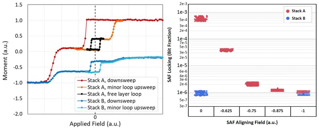
The SAF can lead to yield issues, however – the stack has to be tuned to prevent the SAF having parallel states, which could lock the free layer parallel to the reference layer.
The left-side figure below shows full M-H sweeps for two different stacks, with some samples of Stack A having three stable states under zero external magnetic field. The top half of the plot illustrates the free layer loop from the P and AP states of the free and reference layers under antiparallel configuration of the SAF, and a third state from an (undesired) parallel configuration of the upper and lower layers of the SAF, locking the free layer so that there is no loop. The lower half of the graph shows the results from an improved Stack B, formed so that all of the SAFs had antiparallel configurations, eliminating the third (locked) state. The right-side plot shows the fraction of bits showing SAF locking vs the SAF-aligning magnetic field, confirming that Stack B is resistant to SAF locking behavior.
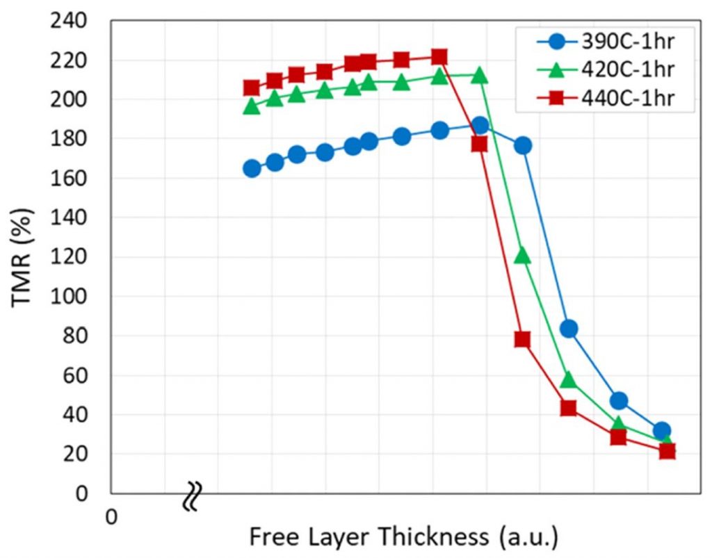
The MTJ can be degraded by high temperatures, so its magnetic properties have to survive through the thermal steps of the backend-of-line (BEOL) processing after MTJ formation, typically an hour at >400°C. In this case, it appears that a higher temperature anneal improves TMR, but there is a critical thickness above which it declines catastrophically;
(RA = 9 ohm-um2)
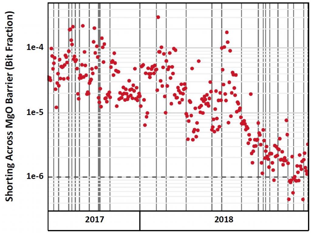
A critical factor in MTJ processing is the quality of the MgO barrier layer, which could be non-uniform, and the MTJ etch could leave residue, both causing shorting; and the top contact could wrap around the MgO, again shorting it out. Below we see the 12-month time trend of Intel’s “Shorting across the MgO barrier” defect indicator, showing that they were able to achieve <1E-6 wafer-level bit error rate due to these defects.
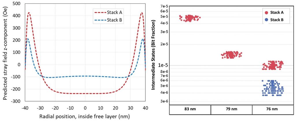
Another problem that Intel had with the integration of MRAM was the existence of states with intermediate resistances, again exhibited by the Stack A formulation. It turned out that the cause was an imbalance of the magnetic fields produced by the top and the bottom halves of the SAF structure, resulting in non-uniform stray dipole fields, shown as simulations of an 80-nm MTJ in the left-side figure below. These stray fields affect the free layer, tipping it towards P magnetization, creating early AP -> P switching in some devices, and forming a metastable structure with P configuration around the layer edges, and AP in the device center. The right-side plot shows the fraction of intermediate states for Stack A vs Stack B with the same device size and matched average stray field, for a range of MTJ sizes; we can see that the effect diminishes with size, and is minimal for Stack B with its reduced stray field. Since stray fields could presumably be a result of unequal etching of the upper and lower SAF layers, it is tempting to speculate that Stack B has an improved etch process compared with stack A, as well as possible different composition. Certainly, in the TEM image they look uniformly etched.
That concludes the yield issues dealt with in the paper. In terms of performance, the write-error-rate (WER) curves show that the switching pulse can be as short as 80 ns, though a larger voltage is needed; longer pulse times tend to a minimum voltage level for complete switching. There is a trade-off for tunnel oxide wear-out between shorter pulse length/higher current, and longer pulse /lower current, putting boundaries of endurance vs WER.
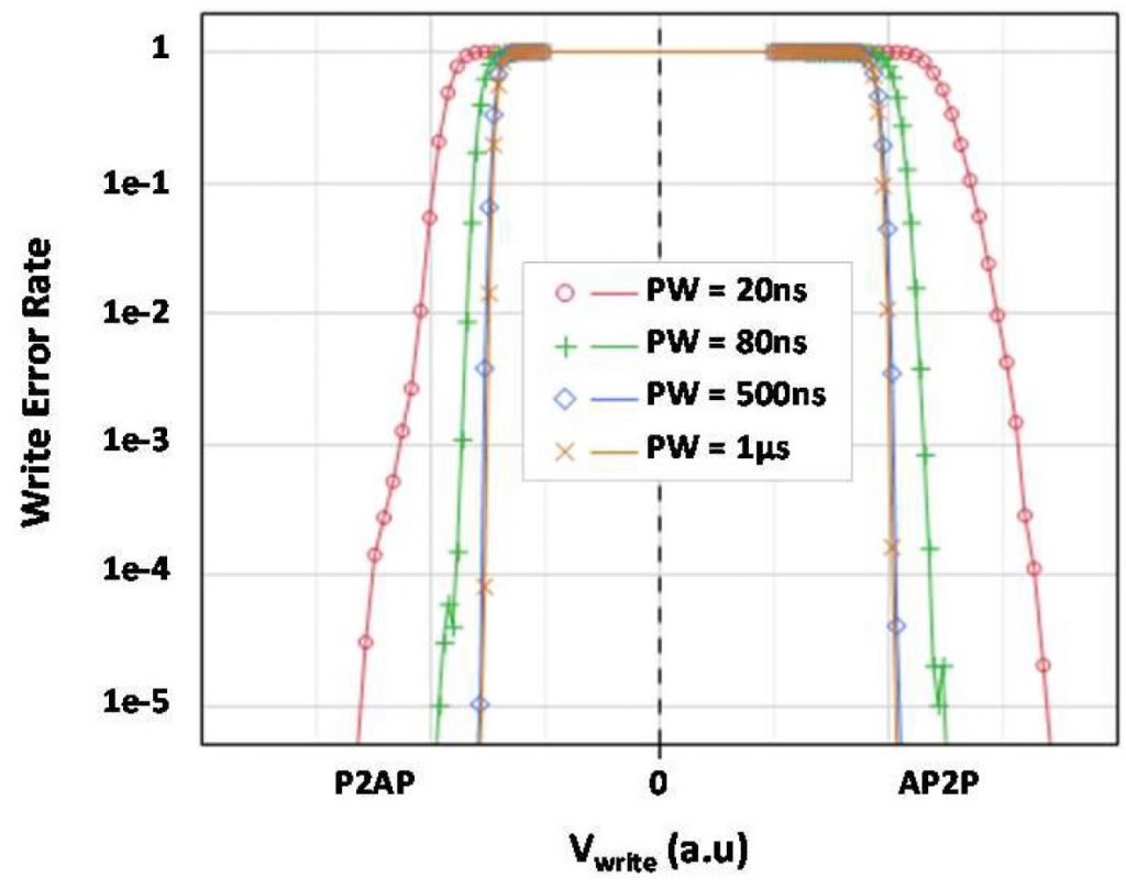
To ensure low WER, an adjustable Write-Verify-Write (WVW) scheme was used, with a series of write pulses of increasing lengths and amplitudes. This can be tuned to trade off write energy vs retention, vs endurance, dependent on the final application. Read sensing is done with a short (<10ns) low amplitude pulse, comparing the current signals between the MTJ and a thin film precision resistor. This can be tweaked to give best read margin, depending on the specific MTJ stack in the final product. (The 22FFL process has a TiN-based MIM capacitor in the BEOL above M4, so one or both TiN layers are likely used for the resistor.)
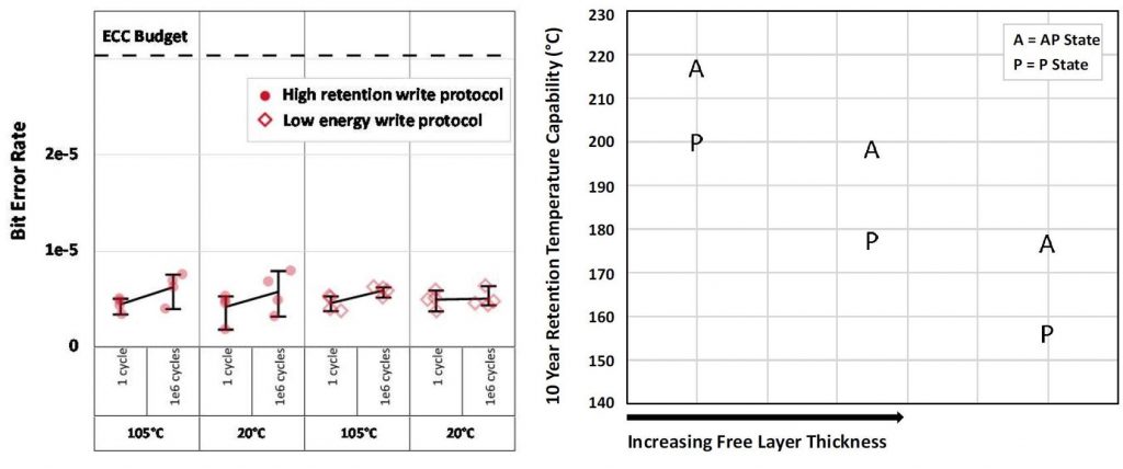
To illustrate the trade-offs that can be made, the left figure below shows the wafer-level bit error rates seen on 7.2-Mbit arrays after 10E6 switching cycles at 20°C and 105°C , with two switching protocols tuned for either low switching energy or high retention. The high retention protocol had a cycling induced fallout rate of <1E-6, and the low energy was <5E-7. The right-side plot demonstrates the effect of free layer thickness on retention properties. The projected wafer-median array-level 10-year retention is plotted for stacks with three different thicknesses, showing 155°C, 175°C and 200°C retention capability depending on the thickness. The projections used raw bit failure rates taken at multiple bake temperatures and times, then extrapolating the data to estimate the temperature for a 1E-5 fail rate after 10 years.
To summarize the whole paper, the MRAM technology uses a 216nm x 225nm 1T-1R finFET cell, with >106 write endurance and 200°C 10-year retention capability, demonstrated in 7.2-Mbit arrays on 300-mm wafers.
References
- O. Golonzka, et al., “MRAM as Embedded Non-Volatile Memory Solution for 22FFL FinFET Technology”, IEDM Tech. Dig. 2018, pp. 412 – 415.
- S. Ikeda, et al., “Perpendicular-anisotropy CoFeB-MgO based magnetic tunnel junctions scaling down to 1X nm”, IEDM Tech. Dig. 2014, pp.796 – 799.