At IEDM last year, Intel gave a half-dozen papers on various topics, including two on their 22FFL SoC process aimed at low power IoT and mobile products. The first (14.1) was an invited presentation on “Intel 22nm FinFET (22FFL) Process Technology for RF and mmWave Applications and Circuit Design Optimization for FinFET Technology”, and the second (18.1) introduced “MRAM as Embedded Non-Volatile Memory Solution for 22FFL FinFET Technology”. I had planned to cover the two papers in one article, but it expanded to the point where it made more sense to split it into two parts. So, here is the first part on the RF enhancements to the 22FFL process.
Part 1 – Initial 22FFL and RF Enhancements
Initial 22FFL Announcements
Mark Bohr announced the 22FFL process at the Technology and Manufacturing Day (TMD) at the end of March in 2017. At the time they said that it was “Fully RF design enabled”, but gave no more details, and MRAM as an option was not mentioned.
More details were given at IEDM 2017 [1], but again no discussion of MRAM. The basic process details as stated at TMD were:
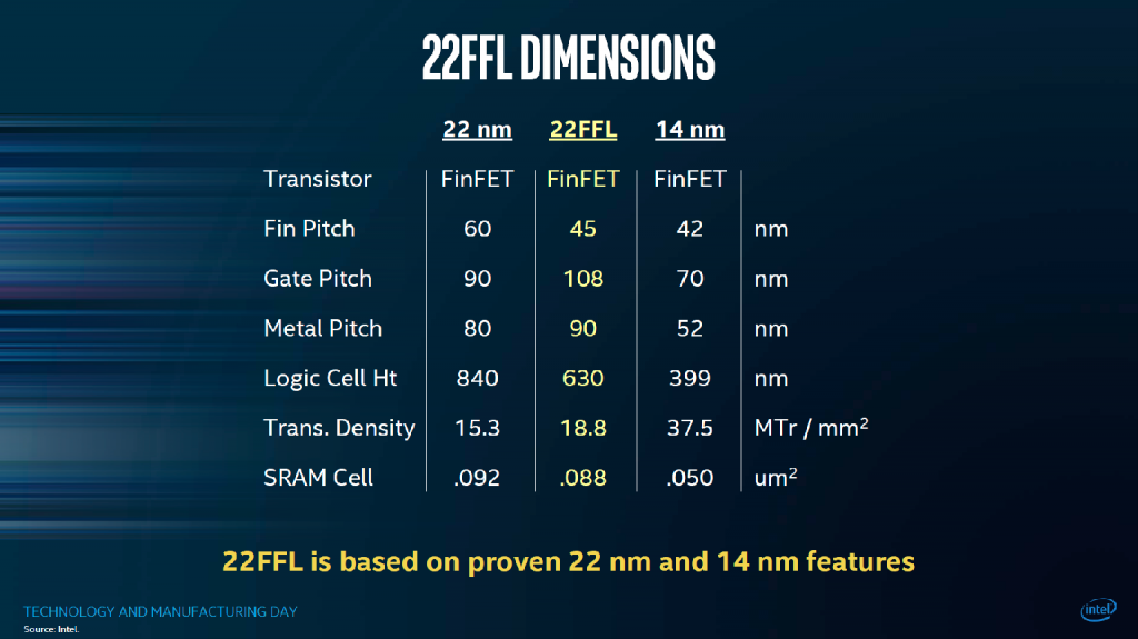
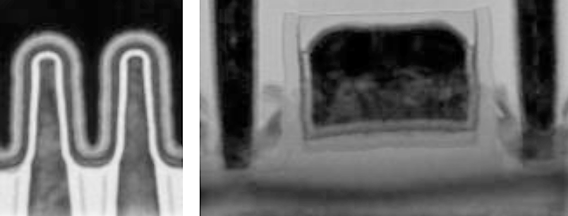
The raw dimensions, as you’d expect, are in between the 14-nm and 22-nm processes. The logic transistor images shown at IEDM17 indicate that 22FFL is based on the 14-nm technology, since we no longer have the tapered fins, and the punch-stop seal is present:
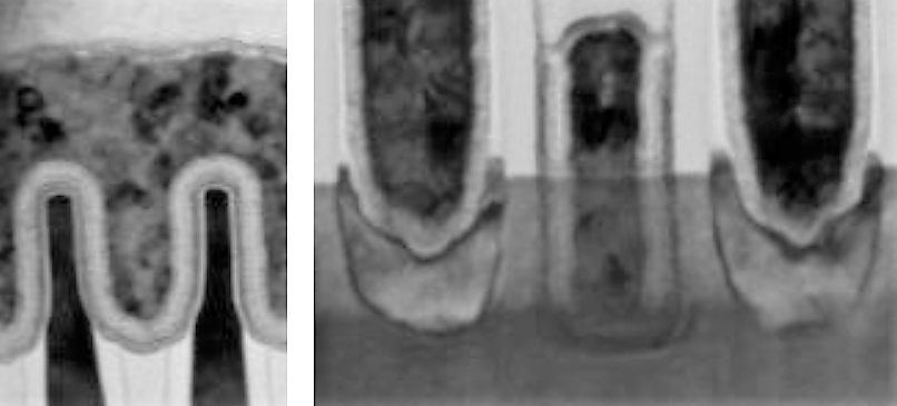
The fins are still double-patterned, but the gate and metal are single-patterned, and the SRAM cell size puts it close to the 22-nm node. If we use the 45 nm fin pitch as a calibration, the fin heights come out at 36 – 38 nm, and fin width ~7 nm, giving a gate width of 80 – 85 nm. That is similar to the 22-nm fins and compares with ~42 nm fin height at 14-nm.
The base process combines high-performance, low power, and ultra-low power logic, analog, and high-voltage (HV) transistors [1]:

The high-performance transistors show 57%/87% higher NMOS/PMOS drive current compared to the 22-nm technology. The use of the punch-stop diffusion means that the fins are undoped, so Vt is set by adjusting gate length and work function for the various devices. As shown in the table, the HV transistors have thicker gate oxide and longer gate lengths.
When it comes to the RF capabilities, a device with optimized layout was developed and showed fT/fMAX of 230 GHz/284 GHz and 238 GHz/242 GHz for NMOS and PMOS respectively, with a 32 nm gate length.
Other SoC features in 22FFL are high resistance substrate, deep N-well isolation, precision resistors, MIM capacitors, and high-Q inductors. The relaxed metal pitch of the single-patterned back end results in reduced parasitics at the sacrifice of density – a good tradeoff for RF SoCs.
RF Modifications
In this year’s RF paper [2], five flavours of transistors were offered;
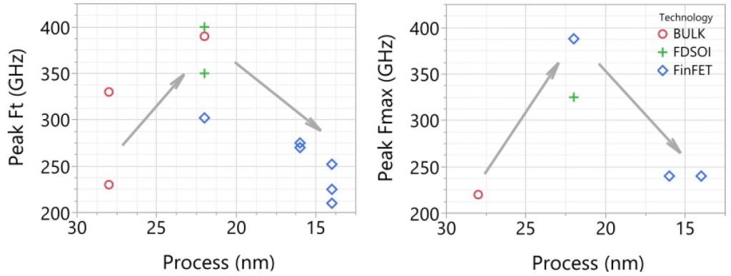
nominal and low VT low-leakage, nominal and low VT high-density, and high-performance (HP). A drawback of FinFETtechnology is the increased lateral parasitic capacitance given by the extra gate material between the fins – as the poly pitch gets tighter, the capacitance increases, lowering fT, without increasing transconductance (gm). This effectively means that the 22-nm process is better suited to RF applications than smaller or larger nodes.
A known phenomenon of finFETs is self-heating, where the fin temperature increases while conducting current, made worse by the thermal isolation of the fin. This impacts temperature-dependent parameters such as mobility and threshold voltage, resulting in performance degradation, and endangering device and interconnect reliability. The effect can be reduced by operating at lower current densities or supply voltages, potentially trading off performance for reliability. Since finFETS have better channel control than planar devices, we can keep strong drive current at low supply voltages, enabling high performance low-voltage designs without reducing reliability.
Another feature of finFETs is the additional vertical component of the gate resistance; this non-linear resistance allows the designer to optimize devices for fT or fMAX by tuning the configuration of fins and gate legs.
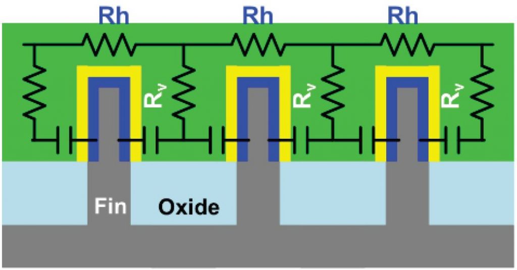
As a result, the HP NMOS fT has been pushed over 300 GHz, and the fMAX beyond 450 GHz, and PMOS to just under 300 GHz.

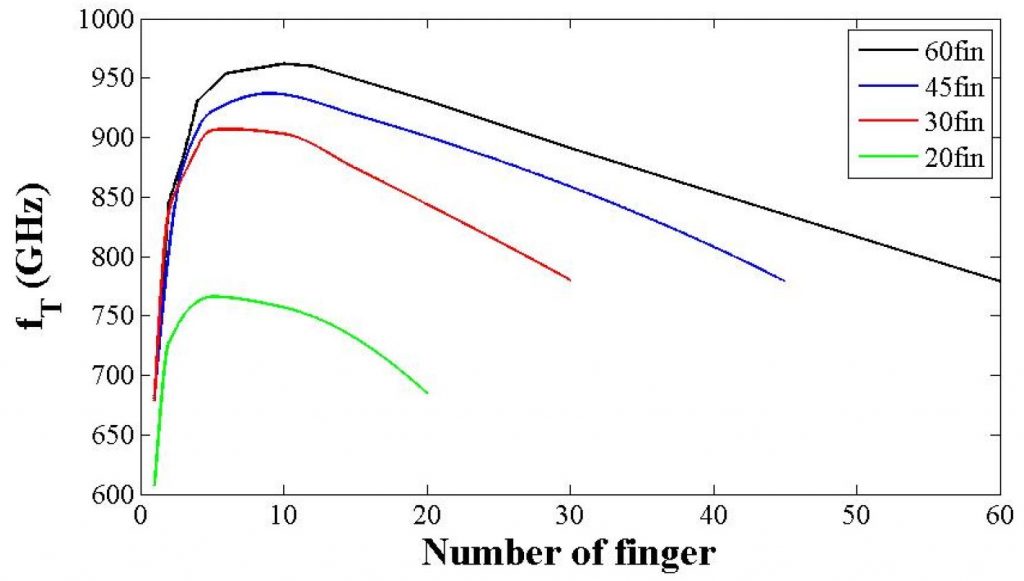
The Intel paper does not give any data on the number of fins or gate legs for the devices described, but I found this simulation [3] based on Intel’s published figures for their initial 22-nm process, i.e. with trapezoidal fins [4]. Using the same effective gate width, it gives an indication of the influence of the fin and gate finger configuration on RF performance. One presumes, looking at these fT numbers (fT >750 GHz for 20 fins), that there are significantly fewer fins in the 22FFL transistors quoted, with an fT of ~300 GHz.
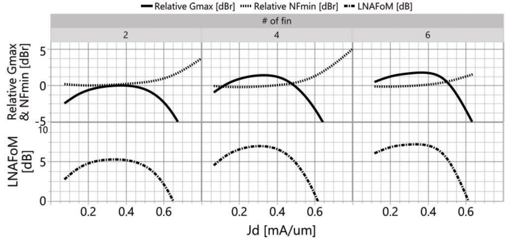
For low-noise amplifier (LNA) designs, noise matching and power matching can be tuned by regulating the input impedance, adjusting the number of fins for a particular device sizing.
Below we see three cases of fin configuration, maintaining total device size by changing the number of gate fingers. The maximum available gain Gmax and the minimum noise figure NFmin vary with the fin number, so the LNA figure of merit (FoM = Gmax – NFmin ) also varies. In this case the FoM maximum is in 4- or 6-fin devices; Gmax and NFmin were normalized to the Gmax and NFmin of a 2-fin device.
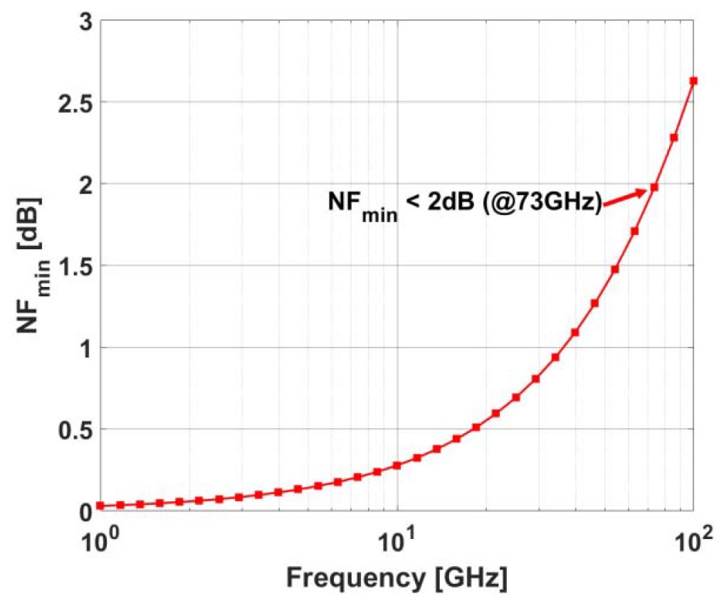
While the above figure shows relative NFmin, other work [5] shows that the noise figure is below 2 dB up to 73 GHz, suitable for a mm-Wave receiver LNA.
When it comes to flicker (1/f) noise, FinFETs have inherently lower drain-induced barrier lowering (DIBL) compared with planar transistors, and we have the punch-through-stop diffusion in 22FFL, so there are no VT adjust implants, and likely no halo implant, both of which help generate flicker noise. By comparison, an equivalent planar transistor is at least 10x greater.
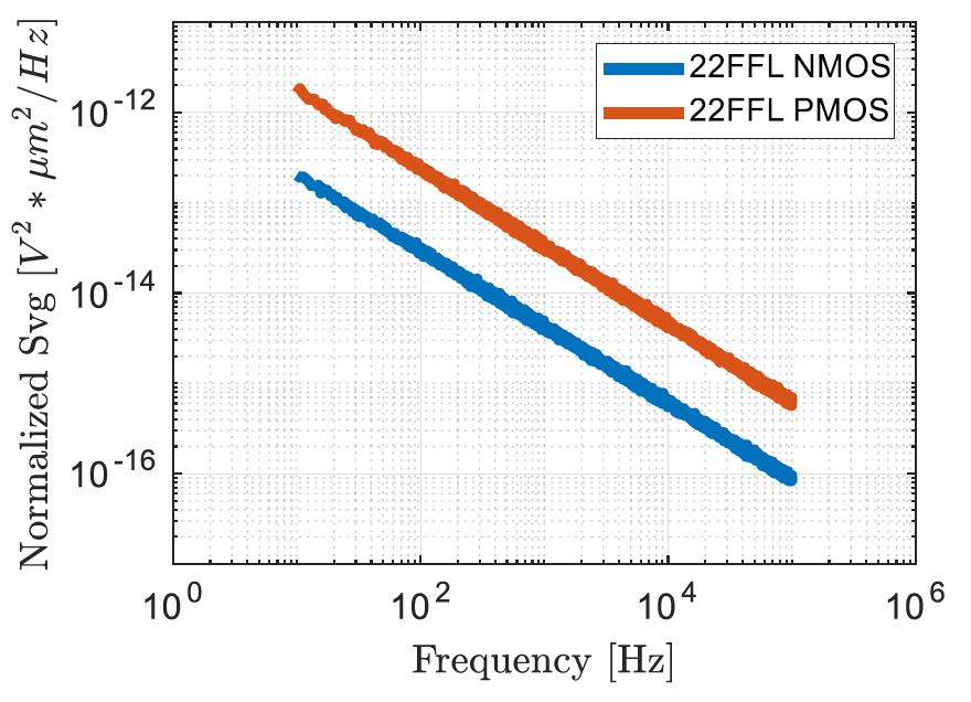
We will see what products come out in the RF-enhanced 22FFL, but with 5G looming up and Intel getting design wins in iPhones, there does seem to be potential, and Intel has clearly been working on the technology.
References
- B. Sell, et al., “22FFL: A High Performance and Ultra Low Power FinFET Technology for Mobile and RF Applications”, IEDM Tech. Dig. 2017, pp. 685 – 688.
- H.-J. Lee, et al., “Intel 22nm FinFET (22FFL) Process Technology for RF and mmWave Applications and Circuit Design Optimization for FinFET Technology”, IEDM Tech. Dig. 2018, pp. 316 – 319.
- T. An, et al., “Performance Optimization Study of FinFETs Considering Parasitic Capacitance and Resistance”, Journal of Semiconductor Technology and Science, vol.14, no.5, Oct. 2014.
- C. Auth, et al., “A 22nm High Performance and Low-Power CMOS Technology Featuring Fully-Depleted Tri-Gate Transistors, Self-Aligned Contacts and High Density MIM Capacitors,” Proc. VLSI Tech. 2012, pp. 131-132.
- S. Callender, et al., “FinFET for mmWave – Technology and Circuit Design Challenges”, Proc. BCICTS 2018, pp. 168 – 173.